
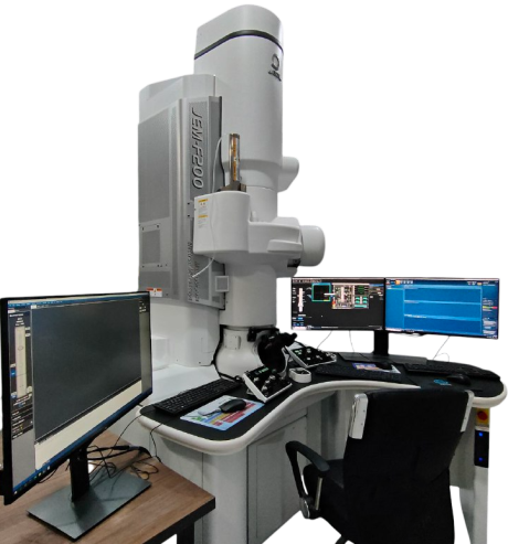
Brand
JEOL (JEM F200)
Description
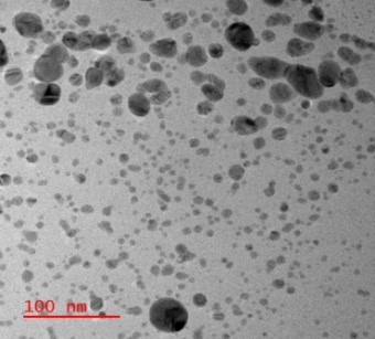
The TEM is more than just a microscope it’s a powerful tool that uses accelerated electrons instead of light to produce high-resolution imaging and analysis of materials at the nano-scale. It can resolve structures down to atomic levels, revealing details invisible under optical microscopes with its advanced features, it enables researchers to explore the structure, composition, and properties of materials with unprecedented detail.
How It Works:
The TEM uses a beam of electrons to penetrate thin samples and produce detailed images.
The process involves:
- Electron Beam Generation: An electron gun emits a beam of electrons. Electrons are accelerated through a high-voltage field.
Sample Interaction: The beam interacts with the sample, magnetic lenses focus the transmitted electrons onto a detector
- Image Formation: Detectors capture the transmitted electrons, creating high-resolution images that reveal structural details.
Applications:
- Material Science: Analyze crystal lattices, defects and interfaces.
- Biology: Study cell organelles, viruses and biomolecules.
- Nano-technology:Characterizenanoparticles and quantum dots.
- Semiconductor Industry: Analyzing thin films and chip components at microscopic scales.
Possible Analyses with TEM:
Structural Analysis
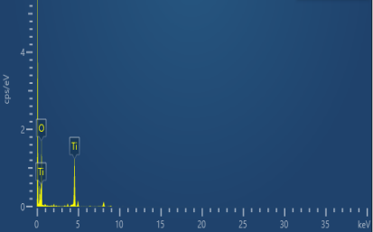
CompositionalAnalysis:
- Energy-Dispersive X-ray Spectroscopy (EDS/EDX).
Electron Energy Loss Spectroscopy (EELS).